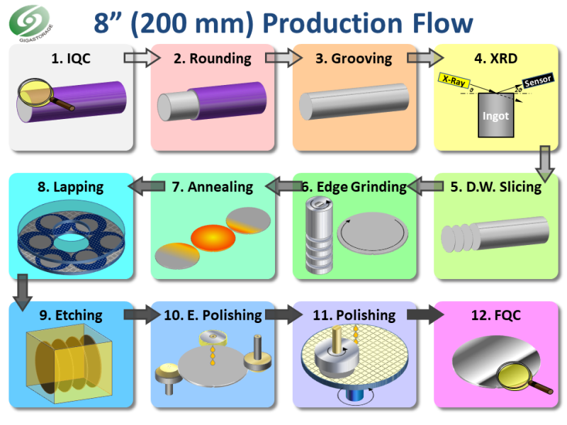

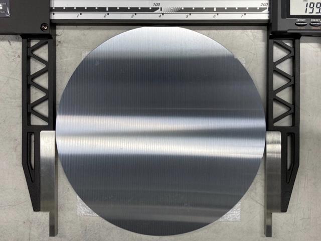
8" (200 mm) Silicon Wafer
- 8" wafer mainly uses for analog chips and novel application chips. Currently, global wafer capacity is around 600 M/month. GIGASTORAGE product 8" (200 mm) semi wafer, we also provide custom service for particular wafers.
 Download
 Contact Us
8" wafer mainly uses for analog chips and novel application chips: Particulate sensor, Driver IC, PMIC , MOSFET, MEMS…etc.
Those chips most apply at smart IoT detector, electric vehicle, and green energy equipment.
Currently, global wafer capacity is around 600 M/month. GIGASTORAGE proceeded 8” wafer pilot run in 2019, verified by customer in the beginning of the 2020.
GIGASTORAGE has faded out solar wafer market in 2018, started R&D 8" semi wafer substrate at same year. In 2019, we proceeded 8” wafer pilot run, verified by customer in the beginning of the 2020.
We expects that wafer capacity can reach 15 Kpcs/month in the end of 2020, further, 30 Kpcs/month in 2021.
GIGASTORAGE product 8" (200 mm) semi wafer, we also provide custom service for particular wafers.
GIGASTORAGE owns a professional R&D team that continues to experiment & develop our technology, and we keep trying to raise the overall yield of process and reduce customer complaint so as to enhance our competitive strength.